Photo: Michael Goss
A special type of single-crystal semiconductor, having part-per-billion purity and high-crystalline perfection, could be the answer to a new type of neutron detector, a device used to detect smuggled nuclear materials or enable neutron-based medical imaging.
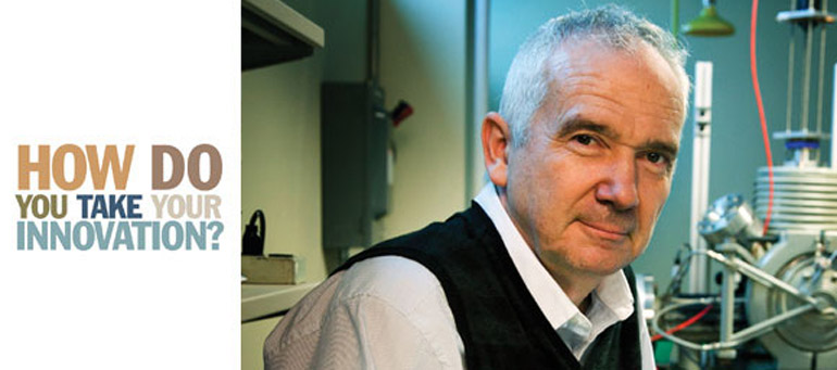
“A crystal,” says Professor Aleksandar Ostrogorsky, holding up a single crystal of germanium, as an example, at his office in University Technology Park at IIT, “is cut like salami into little wafers, which are used as substrates onto which various electro-optical devices are made.” A neutron detector is an example of such a device.
Just as single-crystal silicon revolutionized electronics and computing as the industries’ semiconductor of choice, Ostrogorsky and co-principal investigator Adjunct Professor Glen Slack hope that their slices of monocrystalline boron-6-phosphide (B6P) will provide a much-needed alternative to helium-3, a gas that is the critical component of neutron detectors. These detectors can uncover certain nuclear materials that emit neutrons in addition to more commonly emitted radioactive-charged particles such as X-rays and gamma rays.
The nontoxic, nonradioactive helium-3 isotope was for many years readily harvested as a decay byproduct of tritium, a material used as a booster in nuclear weapons. Due to the decline of the nuclear weapons programs in the United States and Russia, as well as safety issues within the reactors that produced the tritium, the U.S. stopped tritium production in 1998; this has resulted in reduced global helium-3 production to a fraction of the previous levels. According to a Congressional Research Service Report from December 2010, helium-3 demand has exceeded production since 2001.
Ostrogorsky and Slack, both on faculty at IIT Armour College of Engineering, have successfully prepared a high-purity powder form of the compound. Research Associate Ken Morgan, with extensive experience in growing wide band-gap semiconductors, joined the pair last September. Currently, he is trying to melt the powder at temperatures above 2,150°C (4,000°F) to produce a single semiconducting crystal through a slow and precise solidification process. The single crystals will then be processed into wafers, polished and annealed, and used to fabricate neutron-detecting devices.
“If we get good results, there will be many opportunities to commercialize our efforts through a startup,” says Ostrogorsky. “Boron is a superb neutron absorber and we expect B6P to have good semiconductor properties. The question is-can we make a good enough crystal out of it? A 1/16-inch thickness would be sufficient for a good detector. A penny-sized semiconductor crystal could replace the helium-3 gas-filled neutron detectors.”
This project and one at Massachusetts Institute of Technology were the only two university research efforts selected for award under the 2010 Exploratory Research broad agency announcement issued by the U.S. Department of Homeland Security’s Domestic Nuclear Detection Office. In addition to the neutron detector contract project, Ostrogorsky is also exploring a handheld device for detecting X-rays and gamma rays in a project funded by the National Nuclear Security Administration of the U.S. Department of Energy.
More Online
“Helium-3 Shortage Affects National Security, Medicine”: www.pbs.org/newshour/rundown/2011/02/helium-3-shortage-reaches-across-sectors.html