The Answer Man
A
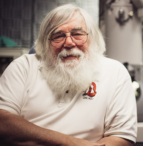
group winds its way down the white brick stairwell of Building 212 on the campus of Argonne National Laboratory (ANL), near west suburban Lemont, Illinois. The voice of one member, Nestor Zaluzec (PHYS ’73)—senior scientist, inventor, and educator—booms out over the sound of equipment as he leads the way next door to the significantly quieter confines of the Sub-Ångstrom Microscopy Microanalysis Laboratory, or SÅMMLab. As Zaluzec unlocks the facility, which sits on a 100-ton concrete base, he can barely contain his excitement. Within SÅMMLab, part of the ANL Center for Nanoscale Materials, is the $8 million Argonne Chromatic Aberration-Corrected Transmission Electron Microscope FEI Titan, or ACAT. But the building’s design is meant to convey even more to come. It is being readied for the arrival of the ng-AEM—“the world’s highest-resolution, highest-sensitivity analytical electron microscope”—slated for delivery in 2018.
“SÅMMLab was specifically built to house the next generation of subatomic resolution instrument, and concepts from it have been adopted in other laboratories around the world,” says Zaluzec. A member of ANL’s Photon Sciences Division, he is a principal figure in the design and implementation of the ng-AEM as well as related scientific instruments and resources at ANL. He notes that SÅMMLab, which he describes as a “building inside a building inside a building,” was an ANL design/build team effort, and its performance has surpassed the team’s design goals. Upon entering one of the microscope rooms, Zaluzec points out waffle-padded walls that resemble a car’s radiator, designed to cool yet minimize the perturbing effects of air flow.
“Each room also has its own vibration-isolation control zone—the microscopes are vibration-isolated from the walls, which are vibration-isolated from the floors, which are vibration-isolated from each area,” he explains. “The rebar used in construction of the floor is made of fiberglass because normal steel material is potentially electromagnetic and can create ground loops and fields. Surrounding the edges of the concrete are two additional vibration-isolation materials—neoprene and foam. Stray external electromagnetic fields in SÅMMLab were low enough that monitors were even able to detect the streetlights turning on and off during commissioning, while the acoustic noise/vibration isolation is under 30 decibels.”
“We’re developing new technologies and methodologies to study nanomaterials in their native states and/or environments."
—Nestor Zaluzac (PHYS '73)
ACAT allows researchers to study materials at a resolution of less than 1 Ångstrom; observing and studying atoms in materials is a routine task in this research instrument. For perspective, imagine that there are about 254 million Ångstroms in one inch and that one million Ångstroms make up the thickness of a sheet of paper. ACAT was the result of a 2004 United States Department of Energy (DOE) project involving a team of national microscopy experts and industry partners FEI and CEOS, and was tailored to examine nanomaterials such as metals, ceramics, catalysts, semiconductors, and superconductors, all at atomic resolution. Zaluzec and other members of the DOE team worked together to design and build the world’s first chromatic and spherical aberration-corrected instrument. The Cs/Cc aberration corrector, the device that enabled ACAT to currently be the world’s highest-resolution microscope, is a series of specially designed electromagnetic and electrostatic lenses, and adjusts for optical limitations typically present in all electron microscopes. ACAT, which is part of ANL’s suite of DOE national user facilities, is accessible to all members of the scientific research and education community.
Another first for Zaluzec’s research group and implemented in the new generation of electron microscopes is the ability to simultaneously examine and chemically analyze by X-ray spectroscopy nanoscale specimens undergoing dynamic processes in liquids and gases. This was previously impossible in electron microscopes because they utilize a vacuum chamber to eliminate air molecules from interfering with the specimen.
The ng-AEM "will not only reach resolutions exceeding ACAT but will also include ultrahigh-spatial resolution spectroscopy and diffraction. It will have a sub-Ångstrom probe as well as the highest-efficiency detectors in the world,” he says, adding that the new microscope will be ideal for extending into the realm of soft matter such as polymers, biological systems, and molecular materials, fields into which Zaluzec is expanding his research interests and efforts.
“We’re developing new technologies and methodologies to study nanomaterials in their native states and/or environments—to study and to ultimately understand how they move, evolve, grow, and change over time," says Zaluzec. "In situ, dynamic, and having atomic-level elemental/chemical sensitivity—that is the next frontier for understanding materials and their properties. And at ANL we will keep pushing that agenda forward, many times at the bleeding edges of R&D.”
The South Side Chicago native says he knew that science was his calling as early as the fourth grade at Oliver Hazard Perry School. But Zaluzec discovered his true niche years later when he obtained a part-time job at the Sherwin-Williams Research Center. Already an Illinois Tech student, he was hired to wash test tubes until managers learned that he had programmed a new calculating machine during his free time to do his homework; Zaluzec was quickly reassigned to tackle analytical challenges. Curious about the light qualities of paint, he designed and built a spectrogoniophotometer dubbed “The Nestorometer” by the Sherwin-Williams lab team.
“That’s where my physics came in,” he says about his academic foundation at Illinois Tech, where, as an adjunct faculty member in the 1980s, he also taught electron microscopy courses. “I had a lot of great professors at IIT, including Earl Zwicker, Fred Ernst, and Tom Erber.”
Word of Zaluzec’s prowess as an inventor and problem solver quickly spread throughout the materials sciences community. He was offered a full scholarship to the graduate program at the University of Illinois at Urbana-Champaign, where he received a Ph.D. in metallurgical engineering and collaborated with acclaimed metallurgist Hamish Fraser. Zaluzec also was honored with the Eugene P. Wigner Fellowship from Oak Ridge National Laboratory, and continues to be a fellow there and in the Computation Institute, established by Argonne and the University of Chicago. In his more than 30-year career, Zaluzec has been recognized with numerous national and international awards, the most recent being the Microscopy Society of America (MSA) 2017 Distinguished Scientist Award for Physical Sciences.
“Nestor Zaluzec’s career has been distinguished by his early recognition and implementation of new technologies and techniques that impact the microscopy field,” says Ian M. Anderson, MSA president, noting that Zaluzec’s contributions include the incorporation of compositional and chemical imaging within a transmission electron microscope (TEM), the early theoretical basis for X-ray spectroscopy in the TEM, and the interpretation of spectra to quantify the composition of nanometer-scale volumes of a specimen. “Even as a high school student, Nestor showed a keen interest in the use of computer technology, and another hallmark of his career was the interfacing of computers and information technology to the electron microscope. A signature accomplishment was the development of what Nestor called the ‘telepresence microscopy collaboratory,’ which enabled the control of microscopy equipment over the Internet, as well as the use of Internet technology for remote collaboration.”
His outreach extends to aspiring scientists. Zaluzec is a member of the Illinois Junior Academy of Science and participates in state and regional science fairs for middle and high school students. Through Argonne he currently hosts the website MicroScape, which gives viewers the chance to use a “virtual microscope” to identify objects at high magnification.
“I do what I do because not only is it important to solve vexing problems in today’s complex and technologically demanding society, but it’s also admittedly fun. I get a little bit of a physical high in the sense that I’ve answered a question and solved a problem. I feel really good about it! And then, it’s like, okay—what are we going to do tomorrow?” says Zaluzec, a youthful joy in his voice. “We need to pass this excitement on to the next generation of scientists.”

Courtesy of Nestor Zaluzec